The WA4DSY 56 KILOBAUD RF MODEM
A Major Redesign
By Dale A. Heatherington, WA4DSY
Abstract
In 1987 I designed a 56 kilobaud RF modem which was sold in kit
form by GRAPES, the Georgia Radio Amateur Packet Enthusiast Society.
This paper describes how the WA4DSY 56 kilobaud RF modem was radically
redesigned to lower cost, reduce size, and improve reliability,
manufacturability and useability. The reader is refered to the
ARRL publication Proceedings of the 6th Computer Networking Conference,
page 68 for details on the original design.
Overview
The original modem was implemented on 3 PC boards. It required both plus and
minus 5 volts for the modem and 12 volts for the external transverter.
The purchaser of the kit had to fabricate his own enclosure and obtain
a suitable power supply. There were no status indicators. Only those hams
with above average home brewing skills would attempt to build the unit.
However, once built, the modem performance and reliability were quite good.
Several high speed networks have been successfully built using these modems.
Unfortunately the large amount of skilled labor required to build a modem
kit and to some extent, the cost have limited the wide spread adoption of
these modems for high speed networking. I have redesigned the modem to
address these issues.
The new design implements the modem on a single 4 layer printed circuit
board powered from a 12 volt power supply. The PC board measures
about 7 inches on each side. Signals produced by the new design are
identical with the original and the new modems will interoperate with the
old ones.
Most of the modem functions are implemented digitally in a
Xilinx (tm)
Field Programmable Gate Array (FPGA). The bandwidth limited MSK
signal is generated digitally at 448 kHz to eliminate the need for analog
double balanced modulators and a 90 degree phase shifter. This signal is
up converted to the 10 meter band at 1 milliwatt. The converter is
synthesized over a 2 mhz range (28-30 mhz). An external transverter
converts the signal to the 222 or 430 mhz band. The delay between RTS
and signal out is quite low, about 20 microseconds or 1 baud interval.
Note that this is a true modem which converts data to RF, unlike the
G3RUH and K9NG designs which are baseband signal processors and don't
do any modulating or demodultating.
The receiver is implemented with a single chip device and is synthesizer
tuned from 28 to 30 MHz. A quadrature detector is used for FM demodulation.
The demodulated signal is sliced using a circuit similar to the one in the
original design which automatically adjusts the slicing level.
The signal is then fed into the FPGA where clock recovery and data carrier
detection are done digitally. The delay between receiving a signal and carrier
detect indication is about 3 milliseconds.
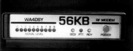
The user interface has been greatly improved. Ten LEDs indicate received signal level.
Other LEDs indicate Request To Send, Data Carrier Detect and Ready.
The data interface is dual mode. A single switch selects CMOS or RS422 modes.
The signals are presented on a DB15 connector wired to mate with the
Ottawa PI2 Packet Interface Card. Other devices such as TNCs can be connected
by wiring an appropriate cable and connectors.
Unlike the original design which allowed the user to reconfigure the modem for
different baud rates, the data rate of the new design is fixed. Major changes
are required to both the RF and FPGA circuits for use at any other baud rate.
Part of the reason is because the first IF of 448 KHz must be 8 (or some power of 2)
times the baud rate. Also, the receiver chip is being operated close to its maximum
rate at 56KB.
Data Coding
All data coding is done in the FPGA chip. The chip is clocked at 14.31818 MHz.
The transmit clock is obtained by dividing by 256. The exact baud rate is
actually 55.9304 kilobaud, the same as the original design. The transmit clock
signal is sent to the user on the RS422 interface. The user's transmit data
source is expected to use the rising edge to clock out each bit. The modem
samples data bits on the falling edge of the clock.
The transmit data stream is scrambled using the same shift register configuration
as the original modem, a 17 bit register with feedback taps at stages 5 and 17.
This is not compatible with K9NG and G3RUH 9600 bps modems. For more details
on the scrambling system, see the section titled "Descrambler" below. After
scrambling, the data enters the digital state machine where both NRZ to NRZI
conversion and RF waveform table lookup operations are performed.
Modulator
This modem has no physical modulator. All RF waveforms are stored in EPROM.
A digital state machine fetches the appropriate waveform segment from EPROM
in response to the current data bit to be transmitted. 32 samples of the stored
digitized waveform segment are read from the EPROM and sent to a Digital to
Analog Converter (DAC) during each baud interval. The carrier frequency is
exactly 8 times the baud rate to permit the splicing of different waveform
segments together without phase discontinuties. The result is a 448 kHz
bandwidth limited MSK signal. Unlike the previous version of this modem,
there are no modulator related adjustment controls. The signal always has
perfect phase shift and deviation characteristics. The signal is identical to the
one produced by the original WA4DSY 56 KB modem.
Transmitted signal characteristics
- Modulation is MSK
- Bandwidth is 70 kHz at 26 DB down
- 3.5 DB amplitude variation
- 14 kHz FM Deviation
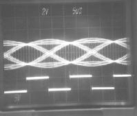
Upper Trace: Unfiltered 448 KHZ Signal from DAC
Lower Trace: 56KB Transmit Clock
Upconverter and IF
The 448 kHz MSK signal shown in the photo above is first filtered with an
80 kHz wide 3 section LC bandpass filter to remove digital sampling noise.
It's then mixed with 10.245 MHz and converted to 10.693 MHz. The 10.693 MHz
signal is passed through two 10.7 MHz (180 kHz BW) ceramic filters to remove
the local oscillator and unwanted lower sideband (10.245 and 9.797 MHz).
The undesired frequencies are reduced by at least 90 db.
The desired 10.693 MHz signal is then mixed with a VCO signal in the 39 MHz range.
The lower sideband of the mixer output (28-30 MHz) is selected with a two
section LC bandpass filter. Both conversions are done with NE602 frequency
converter chips.
The 29 MHz signal is amplified 30 db by an MMIC chip and sent out to the users
transverter on a BNC connector. The output level is adjustable from
-10 DBM to +5 DBM.
The local oscillators are running at all times to assure instant response to
the user's "Request to Send" control signal. The total delay is less than 20
microseconds from RTS to RF data signal out. Contrast this to the original design
which required up to 6 milliseconds to start the transmitter.
Receiver
The receiver uses a Motorola MC13135 chip for all RF signal processing.
The received signal in the 28-30 MHz range from the user supplied transverter
is filtered by a two section bandpass filter before entering the receiver chip.
The first local oscillator is a VCO in the 39-41 MHz range controlled by a synthesizer.
The signal is mixed with the VCO to convert it down to 10.693 MHz.
The signal is bandpass filtered with a single 180 kHz wide ceramic filter
before being mixed with 10.245 MHz and converted down to 448 kHz.
A 60 kHz wide LC bandpass filter provides both selectivity and deemphasis.
Frequency modulation is recovered with a quadrature detector.
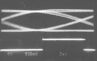
56 KB Receiver Eye Pattern
Frequency Synthesizer
I used a Motorola MC145162 synthesizer chip for this design. It is programmed
serially with a three wire interface. It has completely separate reference
counters and divide by N counters for transmit and receive. The reference
oscillator running at 10.245 MHz also drives both the receive down-converter
and the transmit up-converter.
The VCOs are designed to cover 39 to 41 MHz, 10.693 MHz above the 29 MHz IF
frequencies. The receive VCO is included in the MC13135 receiver chip.
The transmit VCO is a Colpits transistor oscillator with an emitter follower
output buffer.
Since there is no microprocessor in this modem, I needed a way to generate
the data to program the synthesizer. I had the good fortune of having extra
space in the EPROM; so I put the frequency data there. Up to 8 different bit
patterns for independent TX and RX frequencies can be stored in the EPROM.
The first thing the FPGA does after loading its configuration data is read one
of the selected frequency bit strings into the synthesizer chip. Three switches
code for the 8 frequencies. Any 8 frequencies can be programmed into the
EPROM using a simple program written in C. The program will be supplied with
the modem. If the user wants a custom set of frequencies, he must have access
to an EPROM programmer or order a custom EPROM from the dealer. Still, this is
superior to the original design which used custom crystals often requiring a 6 to 8
week wait and costing 10 to 15 dollars each.
Gated Tracking Data Slicer
Before the recovered signal can be used it must be processed to determine the
state of the received bit, 1 or 0. This is done with an analog comparator chip.
Its threshold is set exactly halfway between the voltage level of a "1" and a "0".
It outputs a "1" if the input is higher than the threshold and a "0" if it's lower.
There is a problem when the carrier frequency of the incoming signal changes.
The voltage levels of the ones and zeros change so the threshold is no longer
exactly half way between them. This causes an increase in errors. One common
solution, which doesn't work very well, is to AC couple the output of the
demodulator to the detector. This is fine if the short and long term average of
the number of ones and zeros is equal. This ideal condition cannot be guaranteed
even if a scrambler is used. A much better solution is to put some intelligence in
the detector so that it averages the voltage level of the ones separately from
the average of the zeros and then subtracts the two averages to obtain the ideal
threshold level. This circuit doesn't care about the ratio of ones to zeros as long
as there is a reasonable number of each. A scrambler is used to make sure there
is a reasonable number of both ones and zeros. The circuit will compute the
correct threshold if the input signal carrier frequency is anywhere within the
expected range of the ones and zeros, in this case plus or minus 14 kHz. The
data slicer used in this implementation is gated with the recovered clock. It only
sees voltage levels near the center of a baud interval. A leaky sample and hold
technique is used to grab the middle 1 microsecond of each bit. There is little
variation in the peak levels from bit to bit thus reducing unwanted fluctuations
in the slicing level.
Clock Recovery
Clock recovery is done digitally in the FPGA. There are no adjustments such as
VCO center frequency as in the original design. The phase of a 3 modulus counter
is compared with the data zero crossing times. The counter is driven by a 3.579545
MHz clock. The baud rate for each modulus is listed below.
Modulus   Baud Rate

  63	   56.818  (fast)
  64	   55.930  (on time)
  65	   55.069  (slow)
The counter can divide by 63, 64 or 65. The divide by 64 setting produces a
56 kHz clock. If the zero crossing was late relative to the counters terminal
count then the counter is counting too fast. The counter modulus is set higher
so it will be earlier next time. If the zero crossing is early the modulus is set
lower so it will be later next time. If no zero crossing is detected the modulus
is set to "on time" so the clock won't drift during strings of ones or zeros.
This scheme only introduces about 0.5 microseconds of clock jitter (3%).
Data Carrier Detector
The data carrier detector is also implemented digitally in the FPGA. There are
no adjustments. Two gates are used to separate data zero crossings which fall
within plus or minus 12 1/2% (in sync) of the terminal count of the 3 modulus
counter described above from the zero crossings which fall outside this range
(out of sync). If the clock recovery circuit is phase locked, all zero crossings
should fall within the 25% "in sync" window. This is true even at low signal
to noise ratios. The "in sync" zero crossings cause a 5 bit counter to increment.
The "out of sync" zero crossings cause the counter to decrement.
The "carrier detected" flip flop is set when the counter reaches maximum
count (31). The flip flop is reset when the counter reaches minimum count (0).
The counter is designed not to overflow. It has "stops" at count 0 and 31.
Carrier detect occurs when the clock recovery circuit has acquired phase lock
and 31 more "in sync" zero crossings have occurred relative to "out of sync"
zero crossings. This takes about 3 milliseconds or about half the time of the
original 56KB modem with less falsing. Measurements show solid carrier detect
even when the bit error rate is as high as 6%. Random noise can't assert carrier
detect because the zero crossings have random timings and will occur with equal
probably at any point in the baud interval. Since 75% of this interval is devoted
to decrementing the 5 bit counter, it will quickly go to zero and reset the carrier
detect flip flop. Periodic waveforms that are harmonically related to the 56 kHz
clock frequency will trigger carrier detect if the clock recovery circuit phase locks
to it.
NRZI to NRZ conversion
NRZ is a data signaling format in which zeros are represented by a certain
voltage level and ones by another. NRZI is a signaling format in which zeros
are represented by a change in voltage level while ones are indicated by no change.
NRZI coded data is not affected by inverting the data voltage levels or the
mark/space frequencies in the case of FSK. This modem converts the incoming
NRZI data to NRZ data with a simple circuit consisting of a "D" Flip Flop and XOR
gate. These components are in the FPGA chip.
Descrambler
A self synchronizing data scrambler was used in this modem for two reasons.
First, it makes the data stream look like a random stream of ones and zeros
regardless of the data being transmitted. This characteristic makes the tracking
data slicer and clock recovery circuits work better. Second, it makes the RF
spectrum look and sound like band limited white noise. In other words, the RF
energy is spread evenly over the modems bandwidth and shows no single
frequency lines regardless of the data being transmitted. Any potential interference
to neighboring channels is limited to an increase in the noise floor instead of
squeaks, squawks, and other obnoxious noises. This type of scrambling is also
commonly used in high speed synchronous modems for telephone use.
The hardware to implement the scrambler and descrambler is very simple.
It consists of a 17 bit shift register and two XOR gates, also known as a Linear
Feedback Shift Register (LFSR). Each transmitted bit is the result of the exclusive
ORing of the current data bit with the bits transmitted 5 and 17 bits times before.
To descramble the data, it is only necessary to exclusive OR the current received
bit with the previous 5th and 17th bits. If the data consist of all ones, the
scrambler will produce a pseudorandom sequence of bits that will repeat
after 131,071 clock pulses or every 2.34 seconds at 56 kilobaud.
This linear feedback shift register scrambling scheme does not violate the
FCC prohibition against codes and ciphers because its purpose is to
"facilitate communication" and the algorithm is publicly available.
Note: G3RUH and K9NG scramblers use 17 bit shift registers tapped at
stages 17 and 12. The sequence produced is not maximum length.
8 Bit FIFO and Bit Repeater Mode
To allow this modem to be used as a full duplex bit repeater I have included
a first in-first out (FIFO) buffer and logic circuitry to route the received data
bits back to the transmitter. When repeater mode is enabled, the data carrier
detect signal will assert request to send. A 2 second watch dog timer prevents
transmitter lockup. The FIFO buffer is 8 bits long. To allow for both plus and
minus "bit slip", the FIFO does not start sending data until it's half full.
The transmitter then pulls bits out of the FIFO at it's fixed clock rate while
the receiver inserts bits into the FIFO at the receiver clock rate. The FIFO is
reset when data carrier detect (DCD) drops. With a data rate difference
between incoming and outgoing data of 0.01% a packet of 40,000 bits (5000 bytes)
can be retransmitted before the FIFO buffer overflows. Since this is much larger
than typical AX25 packets, I don't think this restriction will be a problem.
Keep in mind that DCD must drop between packets to reset the FIFO.
A single internal switch enables the bit repeater mode. The external data I/O
connector remains active to allow communication with a local computer.
Watchdog Timer
A 2 second watchdog timer is built in and may be bypassed with a switch setting.
The timer is reset when RTS is false and begins timing when RTS is true.
PTT will be turned off if RTS is not removed after about 2 seconds.
A resistor and capacitor set the time-out value. This is the only analog timing
circuit in the modem.
Remote Control
Computers used in amateur packet networks are often located with the
TNCs, modems and radios in inaccessible places such as mountain tops.
When the computer software crashes, which it often does, the control
operator doesn't want to have to go to the distant site to push the reset
button. A remote control reset function is built into this modem.
Normally open relay contacts are available for whatever use may come to mind.
The contacts close when the modem decodes several milliseconds of a
pseudorandom bit pattern sent to it from another modem in convenient
reach of the control operator. A push button on the rear panel causes the
modem to send the special sequence.
The sequence generator is an 8 bit linear feedback shift register with user
specified taps. The tap locations are specified along with the frequency
data in the EPROM. Each RX/TX frequency pair may have a different code
assigned. Each set of taps produces a unique code. The receiving modem
must see at least 256 bits of the pattern before it will start to close the relay.
The sequence must continue for another several milliseconds to allow the relay
to close. A single incorrect bit in the sequence will reset the decoder so that
another correct sequence of 256 bits are needed to cause relay closure. The
front panel "ready" LED will change from green to red when the code is being
received.
Signal Level Display
Ten LEDs on the front panel indicate relative signal strength. The RSSI signal
from the MC13135 receiver chip drives an LM3914 linear bar graph display
controller chip. I have found this a most welcome feature. I've used it to
map signal coverage areas by first setting my station to "ping" the local 56KB
packet switch every 2 seconds; then with only a modem, transverter and
antenna in the car, I can get a good idea of how well the packet switch
covers various areas by watching the signal level LEDs and the DCD LED
(and the road).
Tune-up and Test Aids
Since only half the EPROM storage was used for the main FPGA configuration
code, state and waveform tables, I provided a switch which allows the modem
to "boot up" using the other half of the EPROM. In the other half is an FPGA
configuration for a direct digital frequency synthesizer which is used to sweep
the modems tuned circuits. It sweeps a 200 KHz range centered on 448 KHz.
A square wave is also generated on the receive clock output line for scope
sync. The rising edge coincides with the 448 KHz center frequency. Adjustment
of the filters for proper response shape requires only a 30 MHz dual trace scope.
The scope must be adjusted so the rising edge of the "receive clock" square wave
is centered and exactly one complete cycle is displayed. The other channel can
then be used to probe various points in the modem to observe the frequency response
envelope calibrated to 20 KHz per horizontal division. The receive filter can be
checked if the an attenuator is placed between the TX and RX BNC connectors.
The transmitter becomes the sweep generator.
A push button on the rear panel will activate the transmitter and send scrambled marks. The 2 second watchdog timer is automatically bypassed to allow transverter tune-up or power measurement.
Interfaces
Transverter: Power and PTT (Push To Talk) transverter signals are provided
on a 5 pin DIN connector. The remote control relay contacts are also on this
connector. BNC connectors are provided for the 29 MHz transverter IF signals.
Pin assignments are as follows:
- PTT
- Relay contact
- Ground
- Relay contact
- +12 volts @ 2 Amps
Power: The power input connector is a common 2.1 mm round
DC power jack used in many other consumer electronic devices.
Positive voltage is supplied on the center pin. A 12 volt 2.5 amp external
switching power supply runs the modem and transverter.
Data: A female DB15 connector is used for the data interface.
The pin assignments are the same as the Ottawa PI2 card. A single switch
on the PC board changes the electrical standard from balanced RS422 to
unbalanced CMOS. The RS422 interface is based on the 26LS32 and 26LS31
chips. The CMOS interface uses a 74HC244 chip.
DB15 Pin assignments
 RS422

1.	No connection
2.	+ Receive Clock 	(out)
3.	+ Receive Data		(out)
4.	+ Transmit Clock	(out)
5.	+ Carrier detect	(out, low true)
6.	+ Transmit Data	(in)
7.	+ Request to Send	(in,  low true)
8.	  Mode Select		(Not Used)
9.	  Ground
10.	- Receive Clock	(out)
11.	- Receive Data		(out)
12.	- Transmit Clock	(out)
13.	- Carrier Detect	(out, high true)
14.	- Transmit Data	(in)
15.	- Request to Send	(in, high true)

CMOS

1.	No connection
2.	Receive Clock 		(out)
3.	Receive Data		(out)
4.	Transmit Clock		(out)
5.	Carrier detect		(out, low true)
6.	Transmit Data		(in)
7.	Request to Send	(in,  low true)
8.	Mode Select		(Not Used)
9.	Ground

10..15 No connection
Internal Option Switch Functions
Switch	   Off		On

1.	RS422		CMOS
2.	Normal		RX Mute Disable
3.	Normal		Repeater Enable
4.	Normal		Scrambler Disable
5.	Normal		Key Transmitter
6.	Normal		Tune up
7.	Normal		Watchdog Disable
8.	Frequency Select 2
9.	Frequency Select 1
10.	Frequency Select 0
Performance
Due to deadline and and other time constraints, I was unable to do a bit
error rate test on the latest PC board revision. The previous version
needed about 2 db more signal to achieve the same bit error rate as
the original WA4DSY 56KB modem. This was a receiver problem related
to excessive wideband digital noise getting into the receiver RF stages.
This will be resolved before production.
Latest Bit Error Rate Test Results  performed after
original deadline .

Test performed on a Rev A modem modified
for Rev B.

                         Errors counted during 18 seconds (1 million bits)

uV	DBM		New Modem		Original Modem

0.56	-112		51091			148077
0.63	-111		26073			 90921
0.71	-110		 8343			 29432
0.89	-109		 1939			  6851
1.0	-108		  443			  1077
1.1	-107		   36			   324
1.2	-106		    0			    82
1.4	-105		    0			    26
1.5	-104		    0			     0
Signal source:
8656B signal generator tuned to 404.650 mhz at +10 DBM mixed
with output of another modem at 28.4 mhz. Mixer output
passes through a variable attenuator. Signal level measured
with Tektronics 7L14 spectrum analyzer with 300 khz BW.
7L14 was calibrated using TR502 tracking generator.
A bandpass filter is required at the output of the mixer
to remove the 375 mhz difference frequency because the
transverter uses a 404 mhz LO and WILL produce an
image in the 29 mhz range.
A single transverter was used with it's output split with
a BNC T connector to drive both modems.
Errors were counted on an HP 5315A counter. Counter was conected
to data output of modem(s). Internal scrambler was used as
the data source. Error counts listed are 3 times higher than actual
raw data errors due to scrambler error multiplication.
Performance with off frequency signals seems to be at least as good as
the original design, degrading only about 1 db with a 5 KHz frequency
offset.
The response time from RTS to DCD has been measured at about 3
milliseconds. I'm using a TXDELAY value in NOS of 5 ms and haven't
encountered any problems. This is much faster than the original design
which required a TXDELAY setting of 15 ms.
The transmitter spectral bandwidth is about the same as the original design.
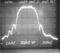
Transmit Spectrum 20 KHz / Division
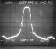
Transmit Spectrum 50 KHz / Division
Applications
This modem can find uses in several areas. When the original modem
was introduced in 1987, the computing power available to the average
ham was quite limited and had problems keeping up with 56KB data.
Today (1995) the average ham can afford a 66 MHz 486 machine.
Multitasking operating systems such as OS/2 and Linux running on
these machines allow hams to set up their own TCPIP Web sites on
the air. Applications such as a Web server are useless at 1200 baud.
For this reason, I believe this modem has as much potential for use as
a user LAN modem as it does for point-to-point links. Assuming the
built in full duplex bit repeater works as expected, I hope to see many
56KB FDX user LANs spring up around the world. They would work just
like an FM voice repeater except for the 70 KHz bandwidth requirment.
There is one such LAN in Ottawa, Ontario, Canada.
We plan to put up a full duplex 56KB Metropolitan Area Network on
222.400 (input) and 223.85 MHz (output) here in the Atlanta, Georgia
area using a 56KB modem, a receive converter, transverter and a
Sinclair duplexer. Users, of course, only need a modem and transverter.
The U.S. now has a 1 MHz wide band (219 to 220 MHz) for
"point-to-point fixed digital message forwarding".
The band is divided into ten 100 KHz channels. This modem
is ideal for that service.
Sales and Marketing
By now you're probably wondering how to get one of these modems.
You can't, at least not right now. The modem is still in development.
However, I'm negotiating with a well known manufacturer of packet
radio equipment to produce and sell this modem. I hope to see them
advertised for sale late in 1995 or early 1996. GRAPES will also be
involved in modem sales.
A Prototype 56KB Modem
You may
download the schematics
of the new 56KB modem. They are in Postscript files compressed with pkzip.
The compressed file is about 64KB in size.
Contact
PacComm Packet Radio Systems, Inc.
for sales information.